
Beamline Phone Number:
+44 (0) 1235 778684
Principal Beamline Scientist:
Dr Gianfelice Cinque
Tel: +44 (0) 1235 778410
E-mail: [email protected]
Email: [email protected]
Tel: +44 (0)1235 56 7675
The MIRIAM beamline B22 at Diamond Light Source has a recently established and unique endstation dedicated to IR nano-spectroscopy/imaging using either scattering SNOM (nano-FTIR) or photothermal contact resonance (AFM-IR or PTE) modes. Both technical approaches benefit from the use of synchrotron radiation (SRIR) as a broadband light source covering the whole IR spectrum.
In addition, single-wavelength nanoimaging is available via QC-Lasers covering the mid-IR fingerprint region.
Nano-FTIR and AFM-IR are two complementary methods for diverse science applications:
Nano-FTIR allows for the highest spatial resolution in IR nanospectroscopy up to 10 nanometre, has a surface sensitivity in the scale of 100 nanometre or better, and measures the complex, spectrally resolved scattering from the sample, where the signal phase corresponds to the IR absorption spectrum in linear approximation. It requires some reflectivity of the sample (or thin samples on a reflective substrate) and the tip is tapping onto it.
Our AFM-IR system using synchrotron radiation can give a spatial resolution around 100 nanometres, is less surface sensitive and ideal for probing the sample properties up to micrometre thickness, with measured signal (amplitude) directly correlated to the absorption spectrum. It relies on some measurable thermal expansion of the sample and the tip is in contact.
The MIRIAM beamline B22 at Diamond Light Source has now opened a dedicated user call for Synchrotron IR beamtime using either scattering-Scanning Near-field Optical Microscopy (s-SNOM) or photothermal Atomic Force Microscopy - IR (AFM-IR).
The deadline for this collaborative user proposals call is 30th June 2024
Specifications
|
Parameter |
Nano-FTIR |
AFM-IR |
|
Spatial Resolution: |
10s of nm |
100s of nm |
|
Sample thickness: |
< 300 nm if on reflective substrate |
ideally > 100 nm up to few um |
|
Spectral range: |
650-4000 cm-1 |
600-5000 cm-1 |
|
Illumination: |
Top illumination |
Top or bottom (transparent substrate) |
|
Spectral resolution: |
> 3 cm-1 (typical 8 to 16 cm-1) |
|
|
Spectral acquisition time: |
1-10 min / point |
|
|
Acquisition modes: |
Whitelight images, Topography, 1D linescans, 2D maps |
|
For these experiments it is essential that users have well-characterised samples. Preferentially, experimental aspects in proposals should be discussed with beamline staff.
All proposals will be assessed based on scientific merit by an independent review panel, with a strong emphasis on technical feasibility including sample-method suitability.
Interested users should submit their application through the User Administration System (UAS) and choose the “B22 commissioning” access route as specific call for beamtime on the new MIRIAM/B22 nano-IR end station.
This call is for beamtime to be allocated between 1st November 2024 and 30th April 2025.
For more information about experiments, please contact Hendrik Vondracek or Mark Frogley.
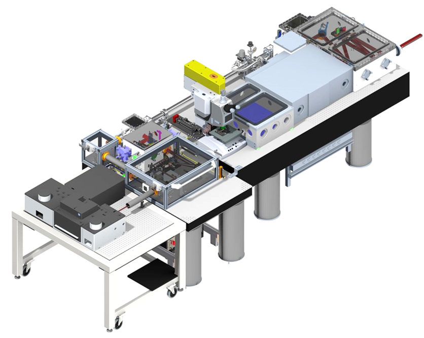
The unique experimental setup at B22 of DLS is based on a customized (Neaspec) IR-neaSCOPE system coupled to a levitation chopper (developed by DLS with Celeroton) and a N2 purged optics box for coupling SR to the system.
A module for s-SNOM, including an asymmetric FTIR interferometer, is operated with SR IR, with the scattered light collected by a high sensitivity MCT detector. The IR spectral range is defined by the detector coverage, the beamsplitter material and the tip-cantilever geometry. For routine experiments on reflective samples, nanospectra between ca. 650 and 4000 cm-1 can generally be achieved. For each imaging measurement, the topography and mechanical response, as well as the IR optical amplitude/phase signal (spectrally unresolved i.e. whitelight) are recorded. Spectra can be recorded in single points or by performing linescans or maps (hyperspectral imaging).
A distinguishing feature of the endstation is the use of SR IR for resonance-enhanced AFM-IR in a separate module, using a symmetric FTIR interferometer. This is possible through a unique feature of our system, a fast vacuum-operated light chopper (up to 200 kHz).The routinely usable IR range for these experiments is from 600 to 5000 cm-1 based on the current setup. This can be enhanced towards higher/lower spectral regions by Si or ZnSe beamsplitters and/or changing the SR IR alignment. The system allows for both top and bottom illumination.
The endstation also features a QC-Laser 4-chip system (MIRCat, Daylight Solutions) which can cover the IR range from about 900 to 1800 cm-1 usable for nanospectroscopy and nanoimaging in s-SNOM (pseudo-heterodyne) and AFM IR modes.
A detailed description of the working principles can be found in the dedicated sections.
In general, suitable samples should fit the following parameters of the AFM stage:
The optical field of view is circa 0.75mm by a 10x magnification optical microscope for sample area identification, by a resolution better than 0.8 µm and a vertical focusing range of circa 250 µm. Visible Images are recorded via a 5 MPixel digital camera.
The region of interest defined by the AFM x-y-z piezo stage is as follow:
Samples must be fixed and adherent to the substrate given the tapping or contact AFM mode of operations. Soft matter matrices are suitable depending on non-contact force. Currently, the system supports samples at standard P and T conditions, including purging by N2 gas for best IR nanospectra.
Suitable substrate and sample matrix depend on the nanoIR method used:
for s-SNOM
For measuring the surface region of reflective samples, the sample can be any thickness up to several mm (cf. above). For low reflectivity samples, the signal can be enhanced with the sample on a reflective substrate - in this case the sample should ideally be less than 100 nm thick. Silicon or Germanium disks and Gold-coated glass substrates work well.
for AFM-IR
In top illumination, the top few microns are generally probed and samples of any thickness up to mm can be measured. The spatial resolution is better for thinner samples, but the signal intensity is then lower, with the ideal compromise being for samples between about 250-1000 nm. Substrates with low thermal conductivity/small thermal expansion are ideal; classic IR transparent materials (CaF2 etc) work well, and are necessary in transmission mode.
Please consider the following guidelines for a nanoIR project:

Diamond Light Source is the UK's national synchrotron science facility, located at the Harwell Science and Innovation Campus in Oxfordshire.
Copyright © 2022 Diamond Light Source
Diamond Light Source Ltd
Diamond House
Harwell Science & Innovation Campus
Didcot
Oxfordshire
OX11 0DE
Diamond Light Source® and the Diamond logo are registered trademarks of Diamond Light Source Ltd
Registered in England and Wales at Diamond House, Harwell Science and Innovation Campus, Didcot, Oxfordshire, OX11 0DE, United Kingdom. Company number: 4375679. VAT number: 287 461 957. Economic Operators Registration and Identification (EORI) number: GB287461957003.

 Soft Condensed Matter